


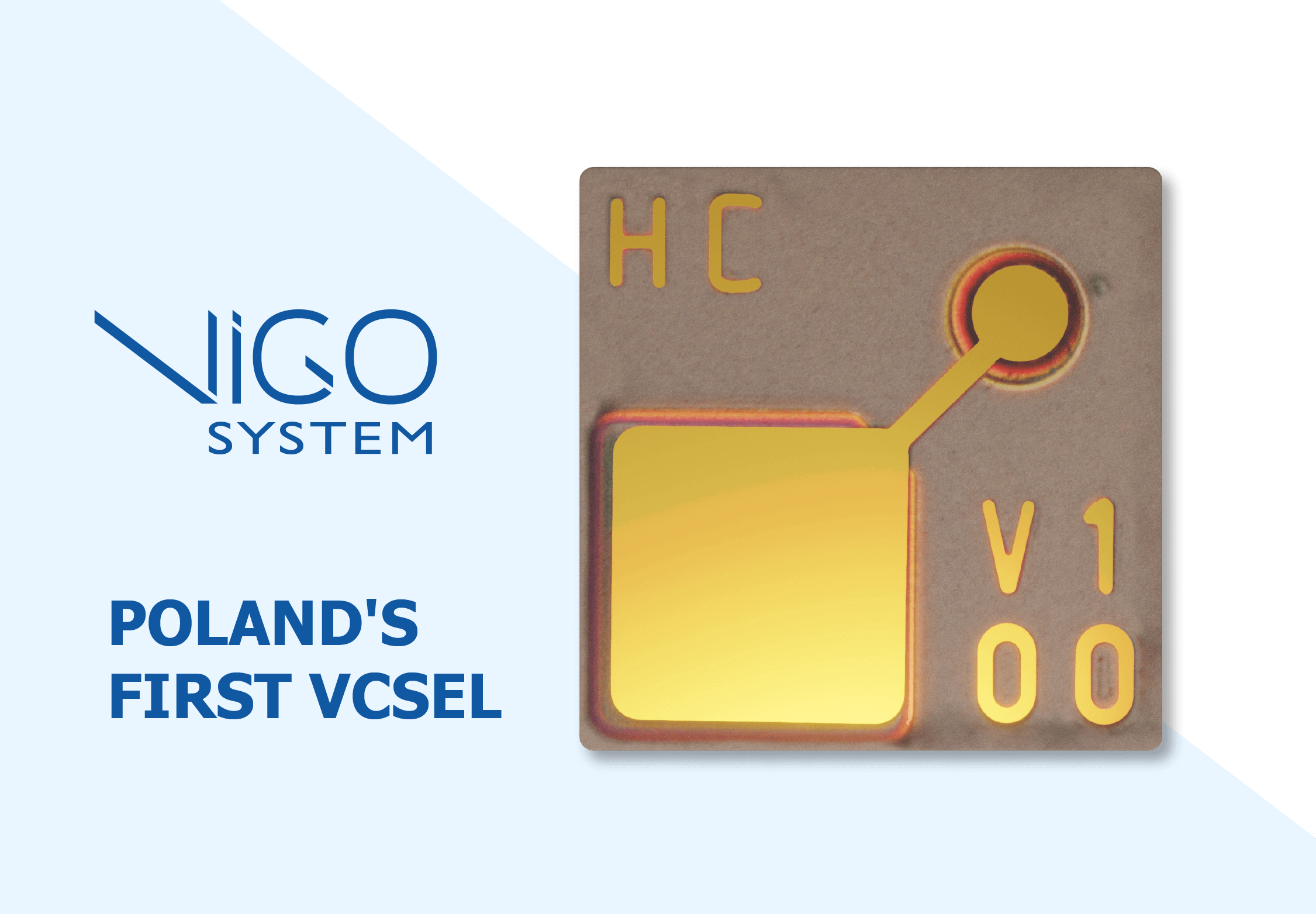
VIGO Photonics, the world’s leading manufacturer of standard and customized high-tech uncooled photodetectors of middle and long wavelength, expands its product portfolio to new innovative epi-structures for vertical-cavity surface-emitting laser (VCSEL). The company has developed its first VCSEL to demonstrate the company’s capability to meet the increasing demand of its customers for disruptive epiwafer technology.
With optical power > 4mW, low threshold current of 0.6 mA and proper spectra characteristics, the 850 nm VCSEL epi-structure is suitable for telecom and datacom optical applications. Compared with other infrared technologies, VCSELs offer highly efficient optical beam, excellent focusing and a very small footprint. Because VCSEL emits light perpendicular to its top surface, a VCSEL chip can be integrated in a single, two-dimensional array, consisting of several hundred individual apertures. Possible applications for VCSEL products are numerous and varied. In addition to communication systems, the devices are used in LIDARs, printers, time-of-flight sensors, autonomous vehicles, robots and drones. Following the successful launch of its first VCSEL epi-wafer, VIGO Photonics intends to increase the production of VCSEL epi-wafers as well as other innovative epi-structures.
The laser device was fabricated within the project „The technology of the production of innovative epitaxial structures and VCSELs” as part of the national programme “Pathway for Mazowsze” (“Ścieżka dla Mazowsza”). The consortium includes VIGO Photonics, as the coordinator of the project, Lodz University of Technology (PL) and Warsaw University of Technology (PW). Wlodek Strupinski from VIGO was responsible for the development of the epitaxial technology, Marcin Gębski from VIGO for the devices processing and prof. Tomasz Czyszanowski from PL for the laser design. The elements of the processing technology were also verified in the Institute of Electron Technology (ITE). It is the first VCSEL manufactured in Poland.
“I am proud that we have been able to launch the production of this complicated structure in just less than six months after starting up the newly purchased AIX 2800 G4 system. One of the greatest challenges was to achieve extremely high precision – with a single nanometer accuracy – in layers thickness control (cavity, DBRs, MQWs) in order to rightly position the resonance dip, as required by demanding telecom applications. The whole epi-structure is about 7 microns thick (which is regarded quite thick) and it consists of more than 200 layers,”– said Wlodek Strupinski, Head of Epitaxy Division.
“This is another future technology that VIGO Photonics is adding to its product line and I am very pleased that our focus on new highly innovative products is paying off. The production of III-V compound semiconductor epitaxial structures for VCSELs and other photonic and microelectronic devices will enable us to further drive long-term profitable growth,” – said Adam Piotrowski, CEO of VIGO Photonics.
More information about VIGO Photonics epitaxy division: