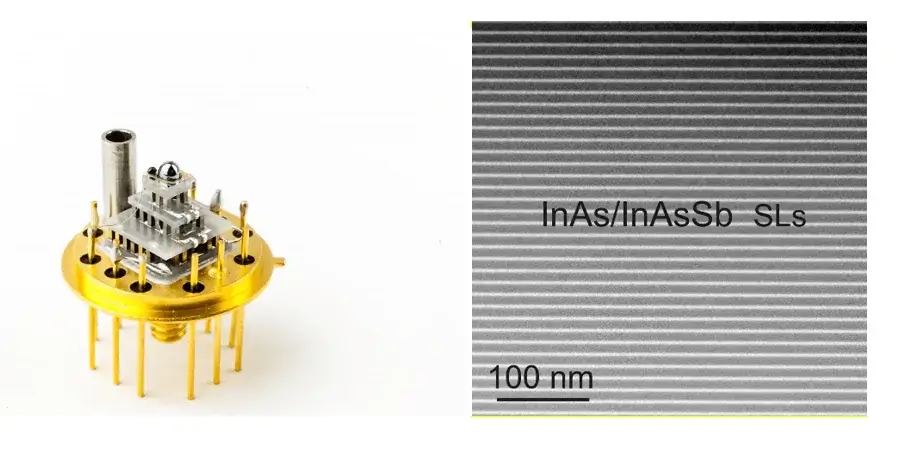
InAs/InAsSb SL Technology
Customers’ demands of wider spectral band absorption detectors in MWIR/LWIR region with competitive parameters to MCT technology encouraged VIGO to develop a novel class of materials & detectors. InAs/InAsSb superlattice (SL) based detectors are our response to fully RoHS compliant product designed for operation with thermoelectric coolers (TEC) at HOT conditions.
Currently manufactured widely used detectors are made with mercury-cadmium telluride compound (MCT) by Metalorganic Chemical Vapour Deposition (MOCVD) technology. Despite many advantages of MCT compound, nowadays in some applications, detectors containing mercury, cadmium and lead are successively removed from the consumer market through norms and directives (e.g. RoHS) due to their toxicity.
Abovementioned limitations connected to MCT encouraged the company to find alternative material system and technology. The InAsSb ternary III-V compound is a great candidate, operating in similar wavelength regime. Encouraged by literature and scientific partners, VIGO decided to develop Ga-free InAs/InAsSb superlattices.
After three years of work on MBE growth technology of InAs/InAsSb SL on SI GaAs substrates, VIGO is ready to present a first generation of SL products with parameters comparable to MCT. So far, we have successfully manufactured photovoltaic devices (MWIR) and photoconductive devices (LWIR).

Advantages
Cut-on wavelength limited to transmission of GaSb buffer ~1.7 µm
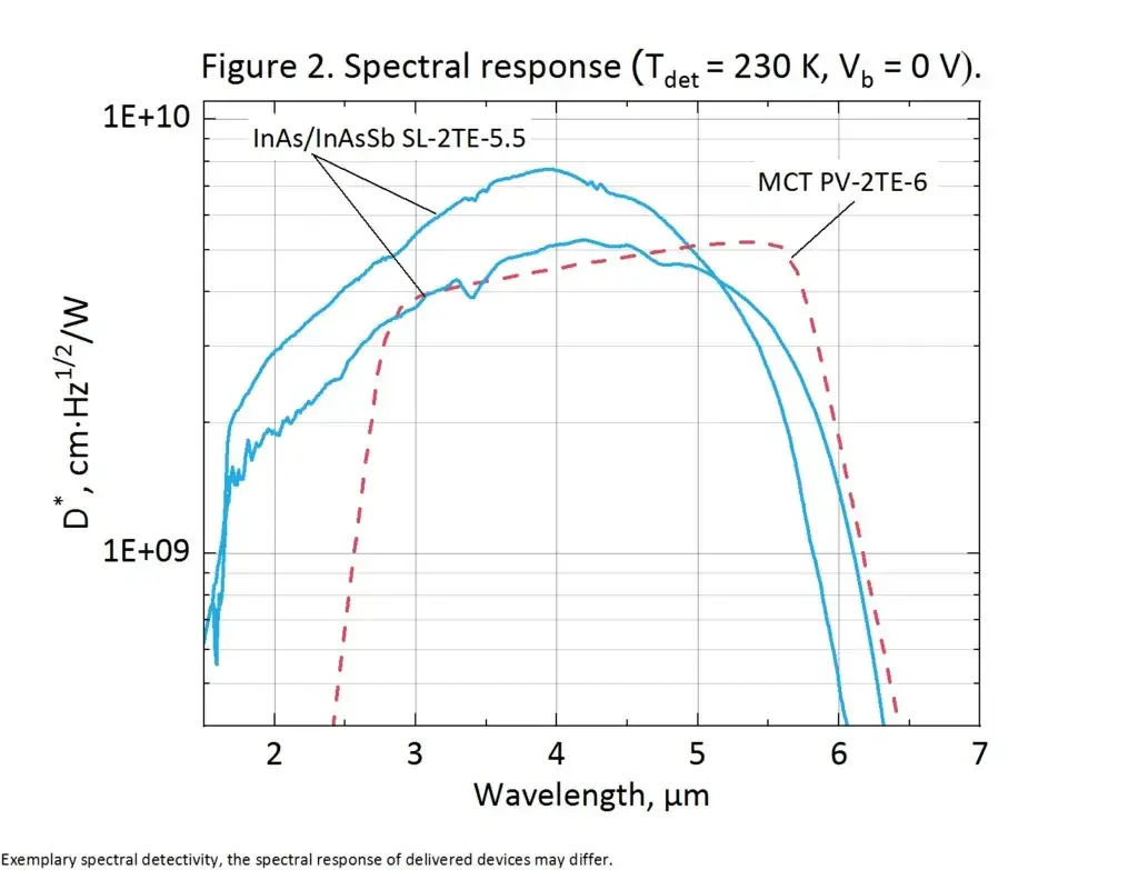
Higher D* compared to PC InAsSb and thermopile detectors
RoHS compliant product
Very good stability ideal for harsh environment
50% cut-off wavelength optimized for 10 or 12 μm
NO LIQUID NITROGEN COOLING REQUIRED! (Fig. 4)
| Parameter | Detector type – Immersed 3TE photoconductive | |
|
Active element material
|
InAs/InAsSb
backside illuminated |
|
| Active element temperature, K | 210 | |
|
Peak wavelength, µm
|
7.0 – 9.0 | |
|
Spectral range, µm
|
1.7 – 11.5 | |
| TO-8 (wZnSeAR) | ~12 | |
| D*(λpeak), cm·Hz1/2/W (@0.5 V) | ~3×10⁹ | |
| Resistance , Ω | >60 |
|
| Active optical area , mm | 1 x 1 |
|
| Package (window) | TO-8 (wZnSeAR) | |