For more than 30 years VIGO Photonics has been manufacturing a wide range of top-quality semiconductor devices for detecting IR radiation within a wide wavelength range (2-16 µm). Two unique features of the detectors sold by VIGO are: possibility to equip them with a monolithic refracting lens considerably improving detector’s performance and ability to work at HOT conditions (High Operating Temperature from -110 °C to 25 °C). HOT conditions are reached using simple to operate thermoelectric coolers what significantly expands the scope of possible applications of the detectors.
Currently manufactured detectors are made from mercury cadmium telluride (MCT) by - Metalorganic Chemical Vapour Deposition (MOCVD), one of the most developed epitaxy techniques. Development of MCT technology started more than a half century ago. At present, MCT is the most widely used variable gap semiconductor for IR market. Over the years parameters of MCT detectors reached the fundamental limits in many applications, but despite that, it also has some drawbacks like poor heat durability, weak mechanical hardness, and hazardous materials used in the manufacturing process. That is why many other material systems are being developed and investigated today, however, MCT technology is a benchmarking point for them.
One of the major interesting competitors for MCT have become III-V materials which manufacturing technology has been improved within the last 30 years. Those materials include metallic group III elements, such as indium, gallium, aluminum, and non-metallic group V elements, like arsenic or antimony. Thanks to their mechanical and chemical properties, they enable manufacturing of detectors with significantly improved mechanical strength, heat durability or resistance to ionizing radiation. The described materials include binary compounds, such as indium arsenide, gallium antimonide, gallium arsenide, indium antimonide and ternary alloys like InAsSb. These compounds and their sophisticated structures (QWIP, T2SL) can cover a wide range of infrared spectrum with excellent device parameters.
Within the last 4 years, VIGO Photonics engineers have achieved many successes in development of III-V materials growth by Molecular Beam Epitaxy (MBE). This method enables deposition of extremely thin layers, down to atomic-thickness. Due to the process conditions, it is possible to deposit multiple thin films with clearly defined material boundaries (sharp interfaces). These properties of the MBE technology open the way to manufacturing devices based on quantum structures, for example, quantum wells.
So far, we have successfully manufactured and implemented photovoltaic devices operating at room temperature or with the use of a two-stage thermoelectric cooler (230 K), optimized for detecting radiation at wavelengths of 3.4 and 5.2 μm with various optical areas, and also with monolithic refracting optics. Such devices are complex heterostructures containing several different materials, including the key absorber material which is InAsSb. Their parameters are comparable with products offered by competitive companies from all over the world. Continuous progress and development of the MBE technology result in increasing repeatability and parameters improvement from one process to another.
While developing growth technology of the InAsSb material, it was also observed that it could be used for detecting a long-wavelength infrared (LWIR) radiation of 12-16 μm. However, parameters of devices manufactured based on this material are not competitive to MCT. In the course of cooperation with domestic and foreign partners, such as the Electron Technology Institute (ITE) or IAF Fraunhofer, their efforts and successes related to development of the type II superlattice (T2SL) technology, based on InAs/GaSb, were observed. Noticing the potential of this direction of development, VIGO decided to start working on superlattices, as well. In-depth literature studies and encouraging preliminary results led to choosing another material system as a candidate for building superlattices - InAs/InAsSb. Easier growth technology and absence of numerous flaws limiting the parameters of InAs/GaSb superlattices sealed the decision on a further development direction of this technology.
A superlattice itself is a system of very thin layers of two materials with a thickness of several nanometers. A single block building the structure is a pair of thin films, for example InAs/GaSb or InAs/InAsSb repeated several hundred times in the depositing process [Figure 1]. Such an arrangement of materials forms, perpendicularly to the deposited layers, a metamaterial showing totally different properties. The properties change due to quantum phenomena related to multiple wells system for both electrons and holes within such structures. In the material manufactured in such way an energy gap can be freely tuned which means that, for example, by changing the layer thickness ratio, one can control the spectral range in which the material will detect radiation.
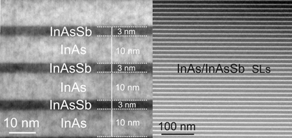
Figure 1
Example of an InAs/InAsSb superlattice structure. Transmission electron microscope images.
Due to their properties and internal structure, T2SL are theoretically capable of showing properties better than those of MCT and can efficiently replace the mentioned material on the market. Such possibility does not seem to be remote in time because today VIGO creates repetitively simple photoconductive devices made of superlattice with a cut-off wavelength of 11- 12 µm with parameters comparable to or even better than those of MCT. It is worth mentioning that superlattices are a demanding material from the point of view of deposition technology, and their parameters, i.e. SRH (Shockley-Read-Hall) generation or short mean diffusion length still differ from the values achieved for MCT.
Nevertheless, the parameters achieved by the InAs/InAsSb superlattices are considerably better than those measured for the InAs/GaSb superlattices at HOT conditions, which was experimentally confirmed by VIGO. Constantly improved technology will enable further improvement of the mentioned parameters, and the next steps taken will result in a development of long-wavelength photodiodes and monolithical multi-cell devices.
Development of the superlattice detectors manufacturing technology is related to the implementation of a research project - TECHMATSTRATEG, the product of which is to be LWIR detectors with a superlattice active area. In the first stage, simple photoconductor devices were developed. Exemplary spectral characteristics compared to MCT has been shown in Figure 2a and detectivity at 210 K of immersed photoconductor on Figure 2b. In the next development stage, heterostructure photodiodes with a more complex architecture will be manufactured, optimized for HOT conditions and LWIR detection.
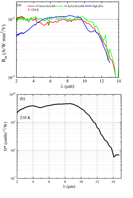
Figure 2
Comparison of normalized spectral current responsivities of photoconductors made of MCT and
of InAs/InAsSb superlattices (a) and detectivity of immersed SL InAs/InAsSb photoconductor (b).
They are inspired by the company’s previous experience from work on similar structures made of MCT. In order to improve the signal-to-noise ratio, the absorber is situated between unipolar barriers layers enabling the flow of carriers generated only by the absorbed radiation. Thanks to the correct architecture of the barriers and the entire heterostructure, as well as a developed technology of material processing, one can obtain a fast device, operating without a bias. Basic results presented for the photoconductors and the time in which they have been achieved instill optimism for the near future. Of course, looking at the path that MCT has gone through to reach the current level of technology and referring to the level of superlattices development, we have to assume that the further development of this material still requires an enormous amount of work. This also means that better and better parameters will be achieved with this material, which will surpass over time the MCT parameters for the LWIR range. VIGO currently has the necessary equipment and staff ready to follow the path of superlattice technology development and its commercialization in the near future.