VCSEL Epi-Structures
At the heart of every high-performing VCSEL lies a precise epitaxial architecture. Grown via advanced MOCVD on n-type GaAs or InP substrates, our custom VCSEL epi-structures combine complex epitaxial engineering with production-ready scalability.
Growing over 200 distinct layers - from active quantum wells to top and bottom DBR mirrors - within a ~7 µm profile leaves zero margin for error. Our industry-leading process achieves accuracy in layer thickness control, locking in the exact resonance wavelength your application requires for maximum efficiency and yield.

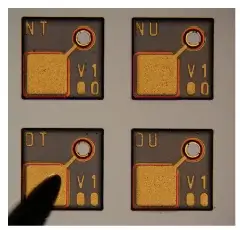
Manufacturing of VCSEL laser die
VCSEL structures have been manufactured successfully on our MOCVD to demonstrate the capability to meet the increasing demand of our customers for disruptive epi-wafer technology.
Compared with other infrared technologies, VCSELs offer highly efficient optical beam, excellent focusing and a very small footprint. Because VCSEL emits light perpendicular to its top surface, a VCSEL chip can be integrated in a single, two-dimensional array, consisting of several hundred individual apertures.