QCLs Epi-Structures
VIGO Photonics’ epi-foundry offers top-quality MOCVD epitaxial growth of a full range of Quantum Cascade Laser structures – we have a long track record of growing designs for numerous wavelengths and applications. To ensure highest growth precision, our epitaxy service includes specially designed calibration methods and a wide portfolio of characterization tools. Thanks to the utilization of multi-wafer MOCVD reactors, the QCL epi-wafers production at VIGO is easily scalable to even very large volumes.
Features of VIGO’s QCL epi-structures:
- High precision of chemical composition (+/- 0.1 %)
- Exact control of layers thickness (+/- 0.1 nm)
- Optimization of the interfaces abruptness
- Low impurities background ≤1E14/cm3
- High repeatability within wafers of the same run and between runs
- High flexibility in applying compounds of different compositions InAlAs, InGaAs and AlAs in the same heterostructure
- High yield and production capacity
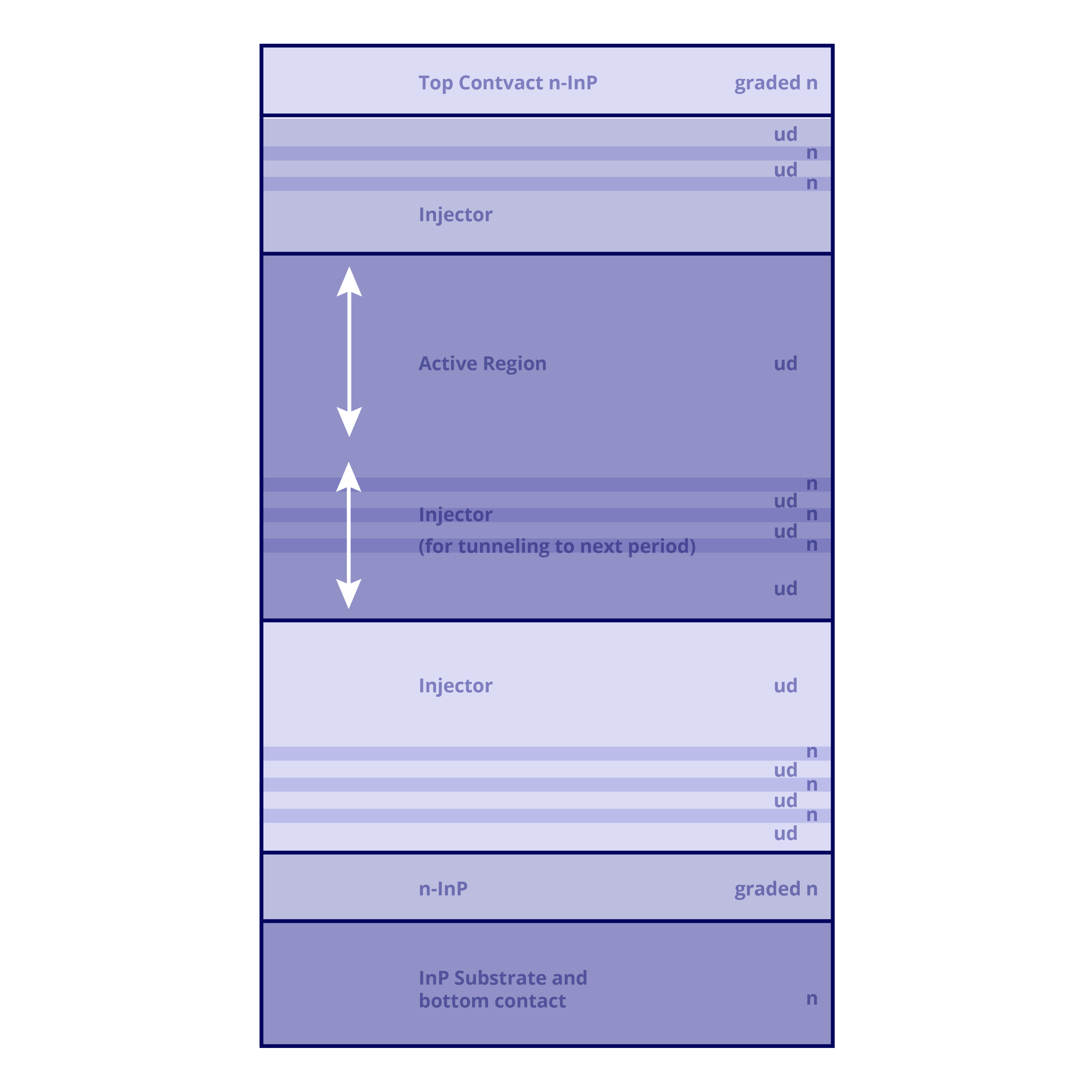
Figure 1. Example of a strain-balanced QCL InGaAs/InAlAs heterostructure. Number of periods 30-70.
Preparation of VIGO’s QCL epi-structures
In QCL structures, the compounds composition and layer thicknesses play a key role in tuning the laser emission wavelength. VIGO’s structures are grown using AIXTRON 2800G4 MOCVD horizontal laminar flow reactor, with the capability of growing epi-layers with exact thickness both within wafer-to-wafer and batch-to-batch comparison. Figure 2. presents a TEM image of a QCL structure’s active region grown by VIGO.
VIGO’s QCL epitaxy process is performed on InP:S (100) substrates at 12 x 2”, 3” or 4” diameter configurations, with 30-70 periods (or even more) of various strain-balanced InAlAs/InGaAs layer sequences sandwiched between thick InP waveguides. The development requires careful measurement of layers thicknesses below critical values. Example of an X-ray diffraction measurement result of strained InGaAs and InAlAs layers is shown in Figure 3.
Structural and electrical properties of epitaxial layers are characterized by X-ray diffraction (XRD), high-resolution secondary ion mass spectroscopy (HRSIMS), optical microscopy (DIC), atomic force microscopy (AFM), transmission electron microscopy (TEM), scanning electron microscopy (SEM), Hall and electrochemical capacitance-voltage technique (ECV).
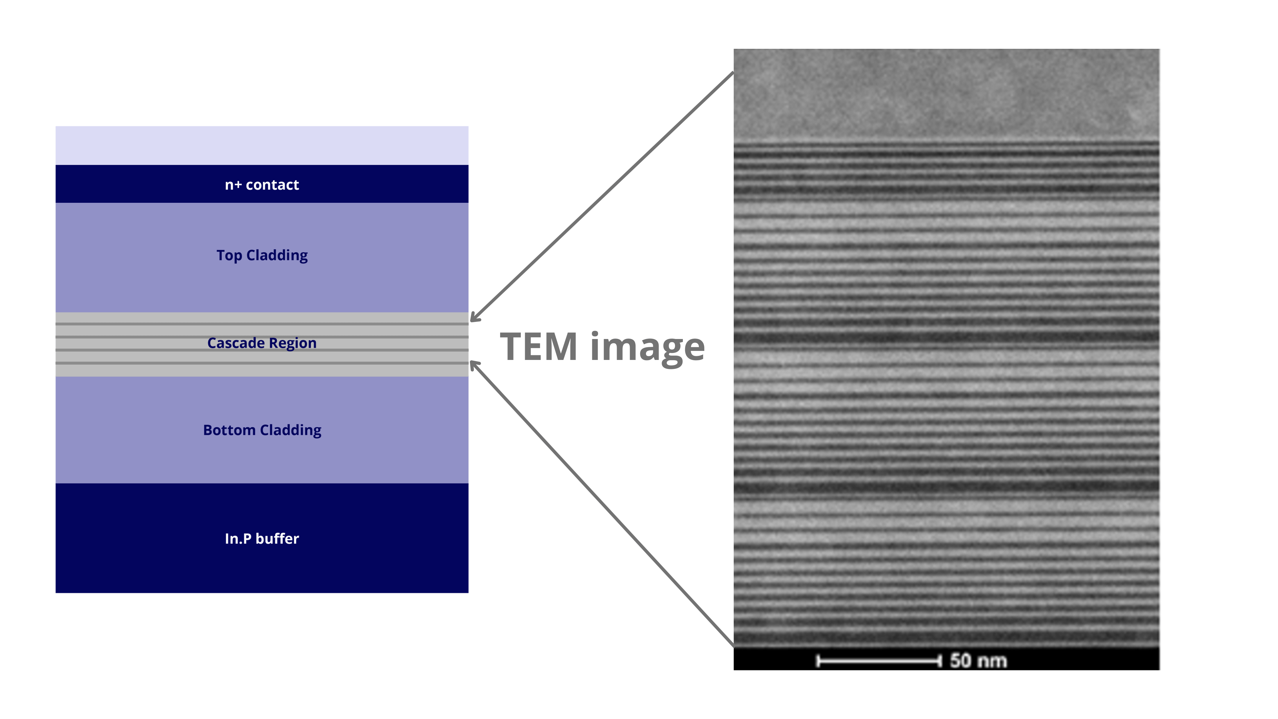
Figure 2. Example of a QCL epitaxial structure with TEM measurement of strain-balanced InGaAs/InAlAs sequences.
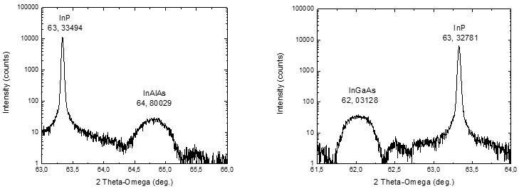
Figure 3. XRD measurement of very thin InGaAs and InAlAs lattice-mismatched and fully strained layers.
Fabrication challenges
Proper preparation and maintenance of the reactor involves deposits control on sensitive graphite susceptors. Paying attention to geometry and positioning of the main rotating planet and satellites is of similar importance. Negligence in any of those activities may lead to worse properties of wafers even within the same run.
In QCLs, the key device parameters such as optical transition energy, wavelength, and electron transport are determined by the epi-structure design. Any discrepancy between the parameters of the grown layers and the specification leads to non-acceptable wavelength change, optical power decrease, shorter lifetime or even no lasing. VIGO’s growth process control results in high crystallographic quality of the semiconductor structure, low impurities background, optimum interfaces abruptness, and stable chemical composition in the several-nanometres strain-balanced InGaAs/InAlAs layers. Such control enables device operation at the expected wavelength and with desired optical power. Figure 4. shows an XRD measurement results of 50 periods of super-lattice obtained in the subsequent growth runs, which proves that high repeatability of layers thickness is possible to achieve in a large epitaxial reactor such as 2800G4.
One of the greatest challenges that VIGO has dealt with is a growth of more than a thousand layers (with a total thickness of more than 10 μm) at the same stable growth rate and - in consequence – with a very well-controlled thickness and composition of each layer.

Figure 4. XRD measurements and theoretical simulations of strain InGaAs/InAlAs super-lattice.
Production of QCL epi-structures requires technology of growing epitaxial layers with mirror-like surface morphology, which can be achieved through carefully optimized growth rate, temperature, reactor pressure, III/V ratio, gases switching sequences, substrate quality and misorientation, as well as impurities incorporation efficiency. A good quality QCL structure is characterized by periodic inequalities. The theoretical scheme of such material property and AFM examination of a QCL structure with 70 periods and 4.5 μm InP waveguide on the top are shown in Figure 5.
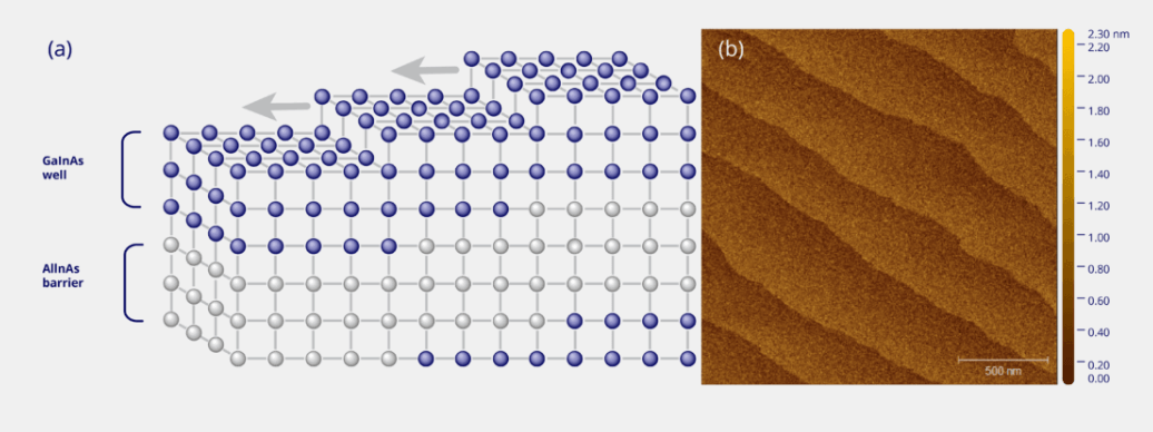
Figure 5. AFM surface inspection of a strain-balanced InGaAs/InAlAs QCL epi-structure.