Choose location

home-icon/Home / About us

VIGO Photonics

VIGO Photonics is a European manufacturer of epitaxial wafers and instruments for photonics and microelectronics, specialized in MWIR and LWIR detectors and modules, produced with the use of internally-developed technology.

37

years of experience

>220

employees

60

marketplaces

6

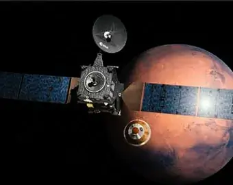
detectors on Mars

VIGO Photonics non-standard solutions allow you to develop products dedicated to customer’s applications:

https://vigophotonics.com/app/uploads/2022/05/Industry-2.svg

Industry

Laser power control and calibration;

https://vigophotonics.com/app/uploads/2022/05/Enviroment-protection.svg

Environmental protection

Gas analysis, real-time water quality control;

https://vigophotonics.com/app/uploads/2022/04/Healthcare.svg

Healthcare

Non-invasive blood analysis;

https://vigophotonics.com/app/uploads/2022/05/Transport.svg

Transport

Analysis of temperature distribution in fast moving objects;

https://vigophotonics.com/app/uploads/2022/04/Industry.svg

Research and development

Precise, non-destructive spectroscopy.

https://vigophotonics.com/app/uploads/2022/04/Defense.svg

Defense and security

Smart munitions, early warning systems.

https://vigophotonics.com/app/uploads/2022/09/Automotive.svg

Automotive

VIGO Photonics is a European manufacturer of epitaxial wafers and instruments for photonics and microelectronics, specialized in MWIR and LWIR detectors and modules, produced with the use of internally-developed technology.

The mission of VIGO Photonics is to provide fast and convenient, easy to use IR detectors at any wavelength from 2 to 16 µm, reaching fundamental BLIP limits without cryocooling. Modules are available with different spectral response ranges, time response characteristics and gains.

VIGO Photonics has a complete front – end and back- end production line for semiconductor high capacity instruments – from epitaxy of II-IV and III-V groups, through detector chips, lasers and their assembly and integration with electronics. The company is constantly expanding its market reach and now has its subsidiaries in the USA.

Strategy
and Mission

The VIGO Photonics development vision assumes strengthening the Company’s position as one of the most innovative
and dynamically developing enterprises on the market.
Our goals include:

  • Exploring the market of MCT (HgCdTe) detectors, including expansion (geographic, segmental) in market areas not covered by regulations, excluding the use of mercury and cadmium in detectors,
  • Advances in the infrared detector technology and infrared modules made of materials based on compounds from groups III and V from the periodic table of elements, in line with the EU Restriction of Hazardous Substances (RoHS) directive,
  • Advances in III-V semiconductor material epitaxy and the production of near-infrared sources (VCSEL lasers),
  • Advances in infrared sources technology,
  • The development of the optoelectronic systems technology and photonic integrated circuits for mid and short infrared,
  • Advances in the infrared detector array technology.
1/4

Technology
of VIGO

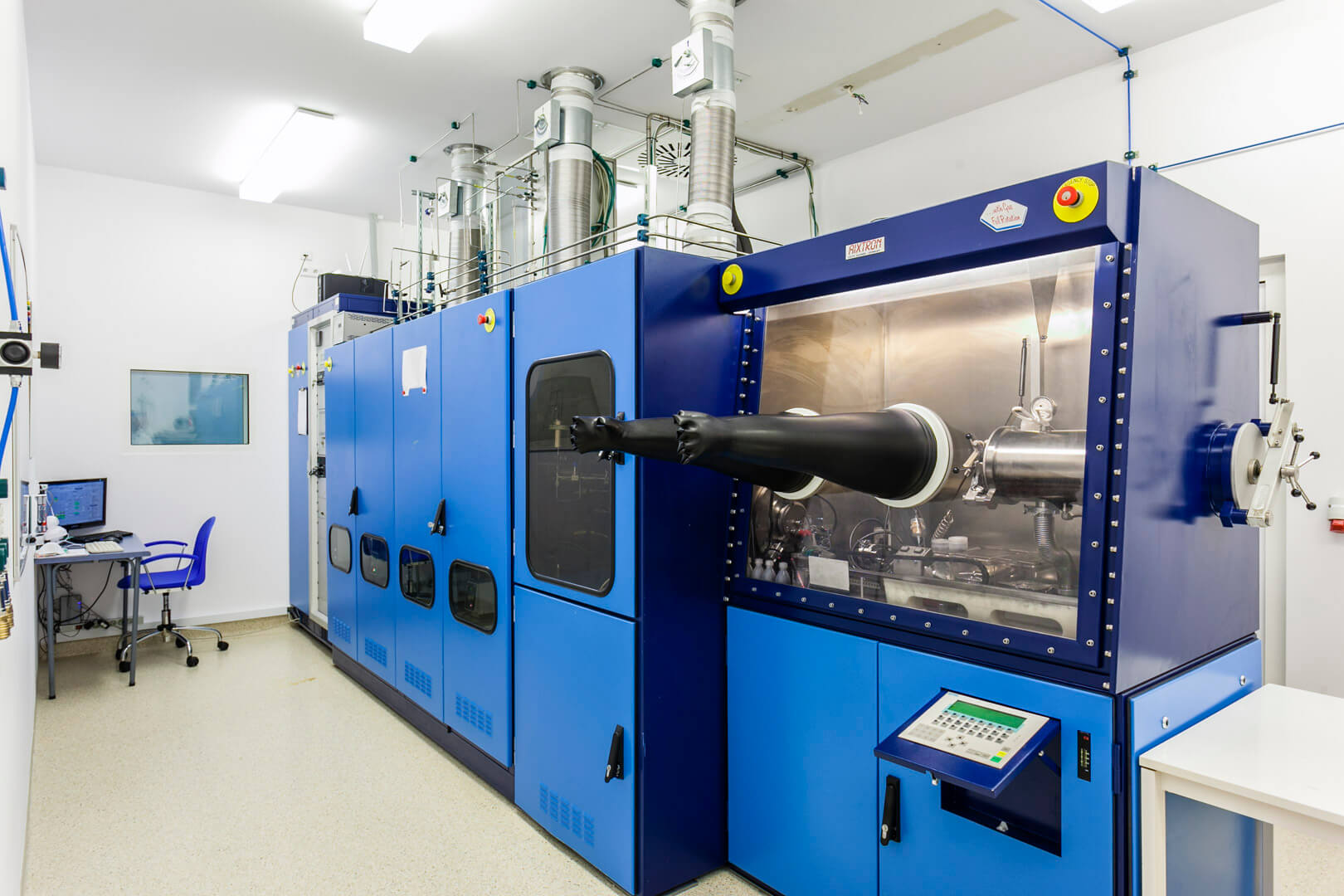
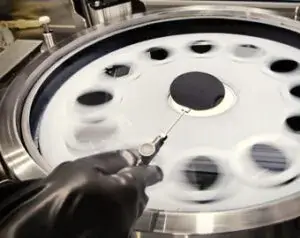
The entire technological process, starting from epitaxial wafer growth, processing, assembly, integration with electronics and measurements, takes place at VIGO Photonics premises.
The techniques used for manufacturing photonics components are following:
- MOCVD – for production HgCdTe MWIR and LWIR detectors and detection modules,
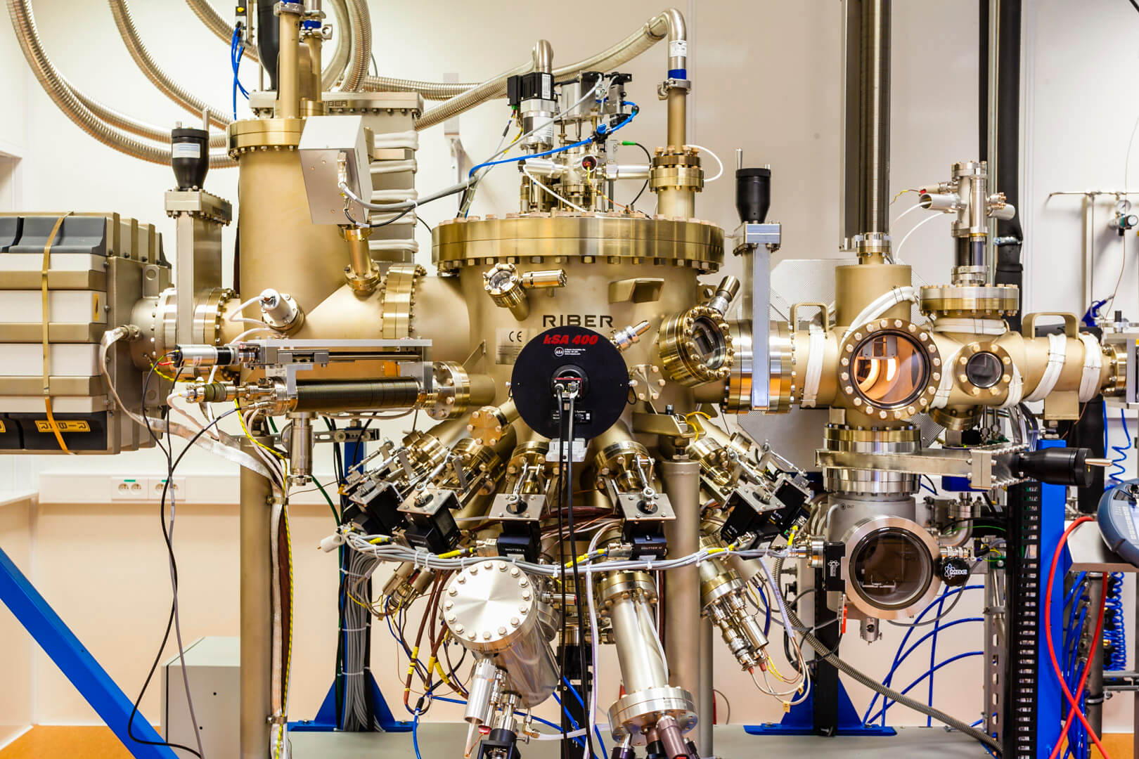
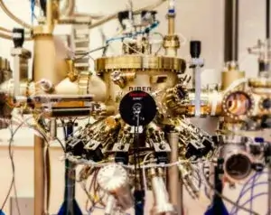
- MBE – for production InAs and InAsSb RoHS compliant MWIR and LWIR detectors and detection modules,
- MOCVD – for production of III-V semiconductor materials for photonic and micro-electronic applications.

MOCVD

The technique used for manufacturing HgCdTe detectors is the metalorganic chemical vapour deposition (MOCVD) method. As a result, multi-layer semiconductor heterostructures are obtained consisting of more than twenty layers as a maximum, varying in terms of thickness, composition, doping and band gap broadening. They fulfil various functions: structural optical, photoelectric and electronic.

MBE

The molecular beam epitaxy (MBE) growth technology is used for manufacturing bulk InAs, InAsSb and superlattice (SL) InAs/InAsSb detectors. SL detectors made of III-V materials have strong covalent bonds, which results in a higher temperature operating range, better uniformity of the crystal, and better optical and electrical parameters.

MOCVD
epi III-V

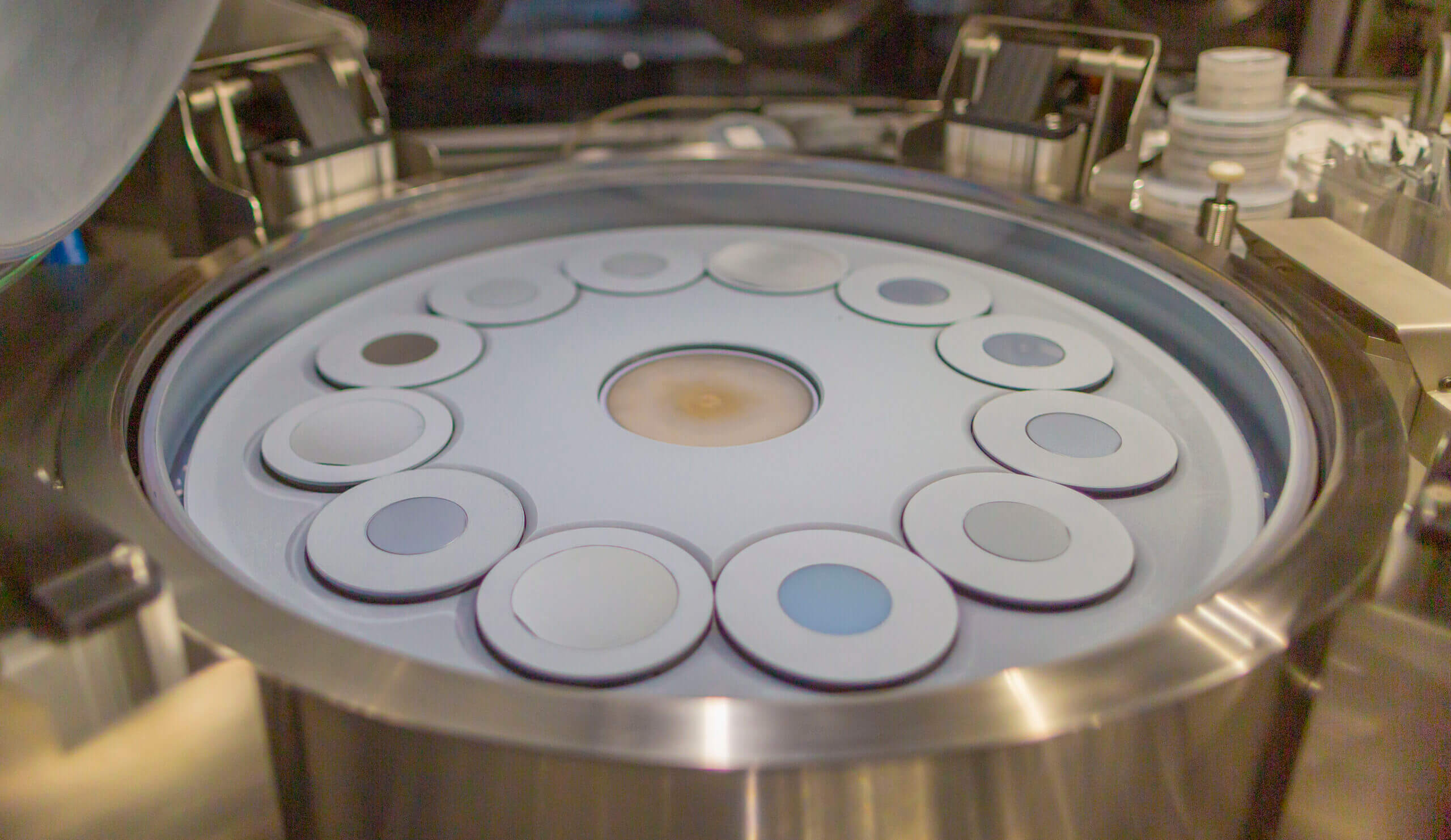
The Planetary Reactor MOCVD is used for manufacturing GaAs or InP based high-quality III-V epitaxial structures for photonic devices (VCSELs, QCLs, photodetectors) and microelectronic devices (diodes, transistors) and others.

Company authorities

Adam Piotrowski

President of the Board

A graduate of Warsaw University of Technology in 2002 with a master’s degree in electronics engineering. A Ph.D. degree in technical sciences engineer at the Military University of Technology in 2008. He works at VIGO Photonics S.A. since 2002. He was introducing novel semiconductor production technologies to the company and managing the production. Since January 2015 is a President of the Board of VIGO Photonics S.A. and as a president of Employer Association Polish Technological Platform on Photonics. Since 2017 he is a member of Board of Stakeholders of Partnership Photonics21 taking active participation european technological development of photonics and microelectronics. He is the author of many publications on methods of manufacture and applications of infrared detectors. He is responsible for application developments of novel sensor systems especially laser based, affordable gas detectors and analyzers. He was taking part in multiple national, european and pure industrial projects.

Read more

Łukasz Piekarski

Member of the Board

Graduate of the School of Economics in Warsaw, Poland and Institute d’Etudes Politiques de Paris, France. He has a university degree in economics and an extensive experience in raising capital for companies and investment projects from European funds, national public funds, as well as in debt financing. He took part in the implementation of a number of investments in the project finance formula. He participated in negotiations with financial institutions and private investors. Since 2014 he has worked as a manager in the Financial Advisory Team IPOPEMA Securities SA where he participated in the implementation of several fund raising projects. In 2006-2013 he was an employee of the Ministry of Regional Development in Warsaw where he was responsible for the implementation of projects financed from EU funds, as well as for the preparation and implementation of pioneering projects, of public-private partnership.

Read more

Marcin Szrom

Member of the Board

Marcin Szrom has gained experience in multinational corporations. His professional career includes working in the semiconductor industry at Texas Instruments in the USA from 2000 to 2012. Between 2012 and 2022, he continued his career in the automotive industry. For several years, he served as Global Director for Advanced Manufacturing Engineering at Kongsberg Automotive, then worked as General Manager at the German company Saargummi. And in the last four years, he held the position of Industrial Engineering Director at VOSS Automotive. He graduated from the Faculty of Electrical Engineering, Automatics, Computer Science and Electronics at the AGH University of Science and Technology in Kraków and completed postgraduate Executive MBA studies at Texas State University in Dallas, USA.

Read more

Investor relations

Regular and transparent communication with all capital market participants is the key to our strategy of building sustainable value for the company on the stock market.

Learn more

History of VIGO

VIGO was founded in 1987, but our history begins as early as 1970 when HOT IR detector technology was created.
Over the years, we have grown and changed just like the technologies we use today because progress is written into our DNA.

1970s

Development of HOT IR detectors technology

1987

Establishment of VIGO Photonics

1992

Speech at the first international fair

1996

The Photonics Circle of Excellence Award

2002

Transformation to joint-stock company

2003

Implementaion of MOCVD technology (joint VIGO-Military Academy of Technology lab)

2007

Relocation to Ożarów Mazowiecki

2012

VIGO detectors on board of the Mars Curiosity rover

2013

Construction of new production facility

2014

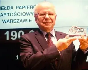
VIGO listed on the WSE

2015

Implementation of MBE technology (joint VIGO-MAT lab)

2016

VIGO detectors again on Mars with Exomars mission

2018

Update of the VIGO 2020 Strategy

2019

The New VIGO Photonics Epitaxy department

2020

New production plant – productivity up to 100 000 detectors annually

2022

Rebranding