In order to ensure a dynamic development, VIGO Photonics runs the Processing 2.0 program. This program is aimed at the development of existing technologies and the creation of new products that will be included in the VIGO portfolio.
As part of the Processing 2.0 program, VIGO runs an investment project entitled “Implementation of the detection chip production technology developed under the “Exposure” project”, under Sub-measure 3.2.2 Loan for Technological Innovations of the Intelligent Development Operational Program 2014 – 2020 co-financed by the European Regional Development Fund.
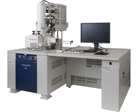
In order to ensure a fast pace of research and development (R+D) projects and improve quality control, it was necessary to expand the capabilities of the measurement laboratories. A significant purchase under the Processing 2.0 program has been a new High Vacuum Scanning Electron Microscope (SEM). So far, the research work requiring the use of SEM investigations had been conducted with the help of longtime partner institutions. On-site research will significantly accelerate the development of both new and existing products.
The purchased microscope is equipped with a cold field emission source (CFE), secondary electron (SE) detectors, and backscattered electron (BSE) detectors. In the near future, it is planned to expand the system with additional detectors allowing for the expansion of research capabilities. Moreover, the SEM is equipped with a loadlock that allows for a quick sample introduction which additionally increases the speed of R+D works. The loadlock is used in combination with a special transfer module which allows to introduce samples prepared by ion milling (satellite equipment purchased in the frame of the same development program) while keeping the sample in a safe vacuum environment. In this way one can ensure no alteration of sensitive samples’ characteristics during transfer to the microscope.
The SEM Regulus 8230 produced by the Japanese company Hitachi in its current configuration allows for the imaging of specimens taking into account material and topographic contrasts. The aim of the measurements will be research and development works and failure analysis of test detectors, and as a result, preventing failures in newer iterations of detectors.
The microscope is also an essential part of the quality control process. In the standard case, after detecting a malfunction of the detector, it was cleaved in order to analyse the structures produced. One of the etching processes was found to be too long, the effect of which can be seen in the micrograph below. As a result, the device does not fulfill its function. The ion etching time was then reduced to improve the process.

VIGO is working on implementing Vertical Cavity Surface Emitting Laser (VCSEL) lasers into production. The key element in the production of these lasers is the aperture which is created by the oxidation of one of the layers.
The oxidized part of the layer will be darker in the microscopic image. In the picture below one can see that the layers oxidize at different rates and one of them oxidizes faster which is a deliberate process and a way to create the aperture.


EXPENDITURE CO-FINANCED BY THE EUROPEAN REGIONAL DEVELOPMENT FUND
POIR 03.02.02-00-1638/18-00
