VCSELs epi-wafers
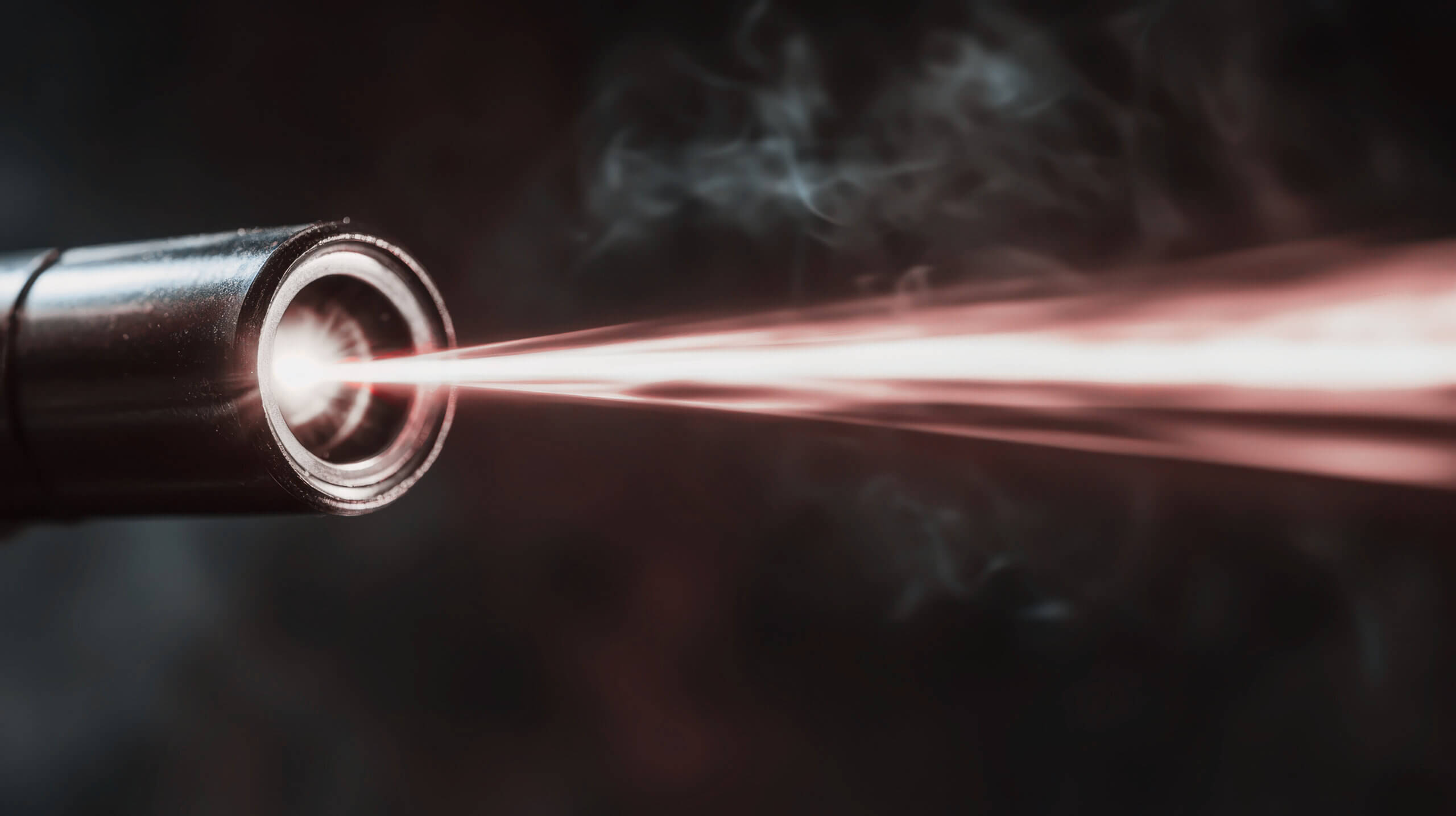
The VCSEL structure, grown using MOCVD technique, consists of a thin multilayer stack with a Fabry-Perot cavity containing quantum wells, enclosed by top and bottom Distributed Bragg Reflectors (DBRs).
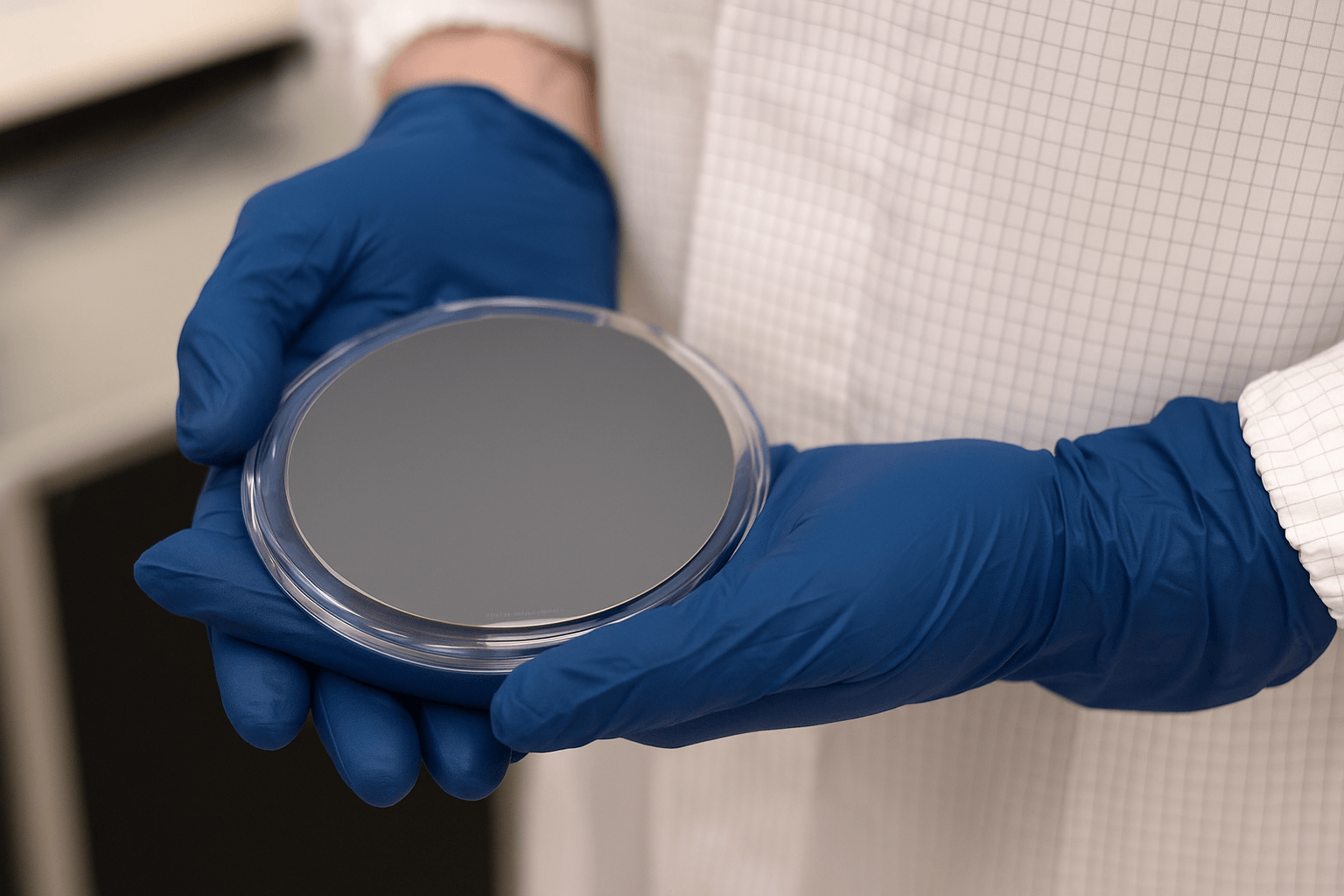
A VCSEL epi-wafer refers to an epitaxially grown semiconductor wafer designed for the fabrication of Vertical-Cavity Surface-Emitting Lasers (VCSELs). It features a layered structure that includes an active region placed between two Distributed Bragg Reflectors (DBRs), composed of alternating semiconductor layers with high and low refractive indices. This vertical cavity design enables emission of light perpendicular to the wafer surface, resulting in a circular, low-divergence beam that is easy to couple into optical fibers and ideal for integration into compact, high-density arrays.
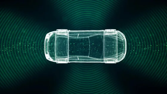
VCSEL epi-wafers are a key component in a wide range of industries, including data communications, automotive (LIDAR and driver-assistance systems), consumer electronics (3D sensing, facial recognition), industrial automation (optical metrology, position sensing), healthcare (biosensing and imaging), and printing technologies.
Similar applications